Guadaloop Wireless Power Transfer
A dynamic wireless charging track that powers a moving pod across a 100 mm air gap. It's designed for 1.2 kW at 60 V, simulated end to end in MATLAB/Simulink, with a synchronous MOSFET rectifier board for the receiver in progress and being simulated in LTspice.
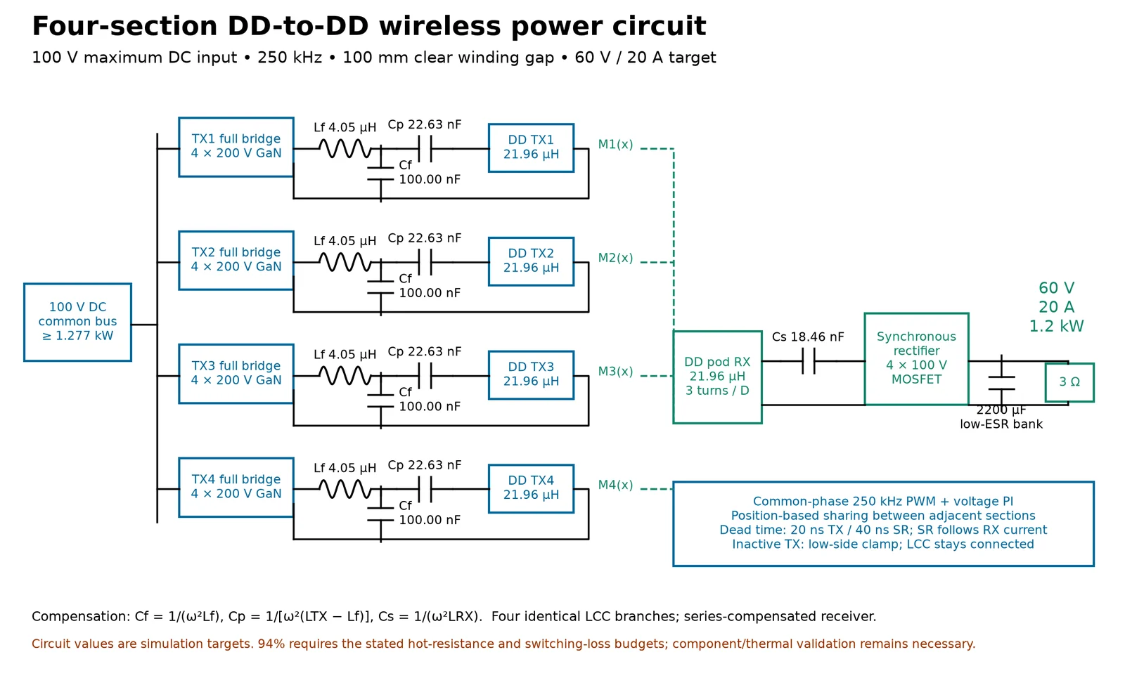
System design
- Track
- 12 × 2 ft: four 3 × 2 ft sections, each with its own DD transmitter pad
- Receiver
- One matching DD pad on the pod
- Input / output
- 100 V DC max in; 60 V, 20 A, 1.2 kW out
- Compensation
- LCC on each transmitter, series capacitor on the receiver (LCC-S)
- Transmitters
- Four GaN full bridges (16 × EPC2304) driven by LMG1210 gate drivers
- Control
- Shared 250 kHz timebase; adjacent sections share power by position as the pod crosses a seam; voltage PI loop
- Receiver rectifier
- Synchronous full bridge that switches with the receiver current instead of using diodes
Coil design
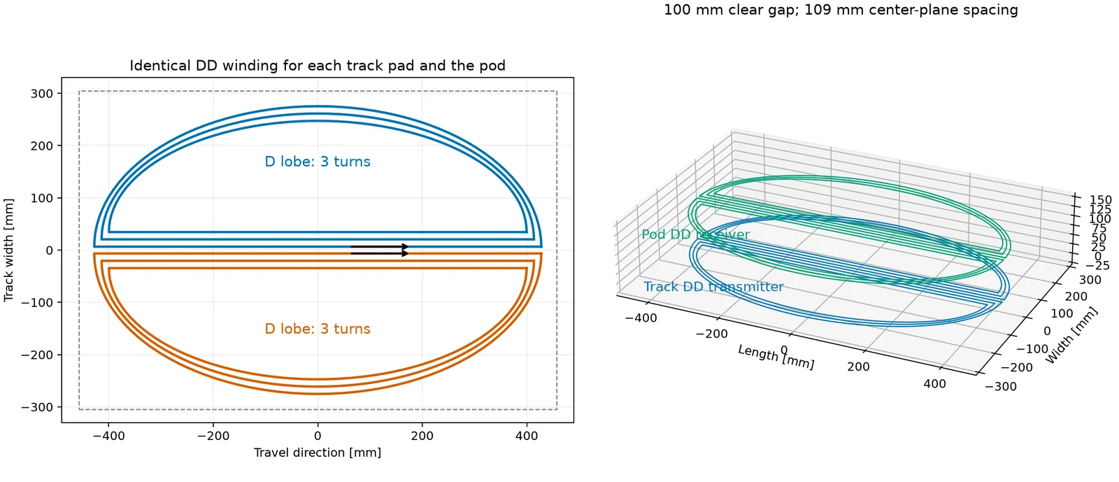
- 21.96 µH per pad; coupling 0.21 when aligned across the 100 mm gap.
- Inductances computed with a Neumann line-integral field model, including every pad-to-pad coupling.
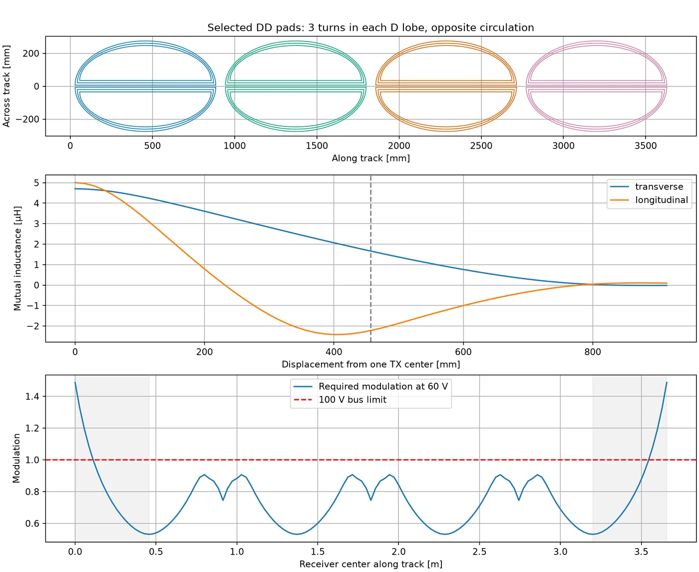
- Pads are oriented so neighboring sections overlap with the same sign, letting power hand over smoothly at each seam.
- Litz wire (about 6,000 × 42 AWG strands) to limit 250 kHz losses.
Simulation results
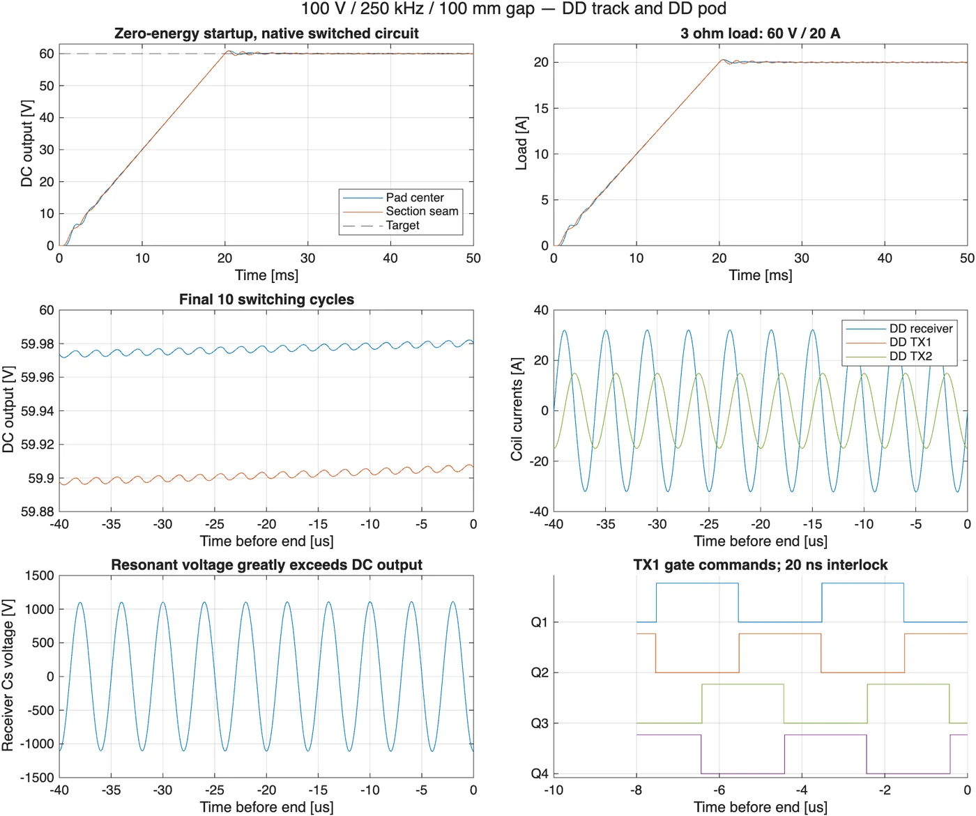
Full switched-circuit Simscape runs with all five windings and 20 semiconductor models. From a cold start, every tested position on the track settles at 60.0 V and 20.0 A within about 20 ms, with an estimated 95.0–95.4% DC-to-DC efficiency.
| Pod position | Output | Est. efficiency |
|---|---|---|
| Over a pad center | 60.0 V · 20.0 A | 95.0% |
| Over a seam between sections | 60.0 V · 20.0 A | 95.4% |
| Hardest point to drive | 60.0 V · 20.0 A | 95.4% |
| Track entrance (half off the track) | 40.3 V · 13.4 A | 94.2% |
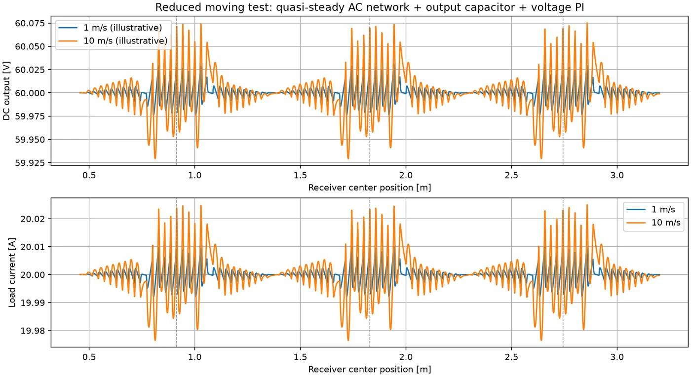
Note: These are simulation results. The coils still need to be built, measured and tuned at 250 kHz, and the receiver's resonant capacitor sees about 1.5 kV even though the output is 60 V.
Synchronous rectifier PCB
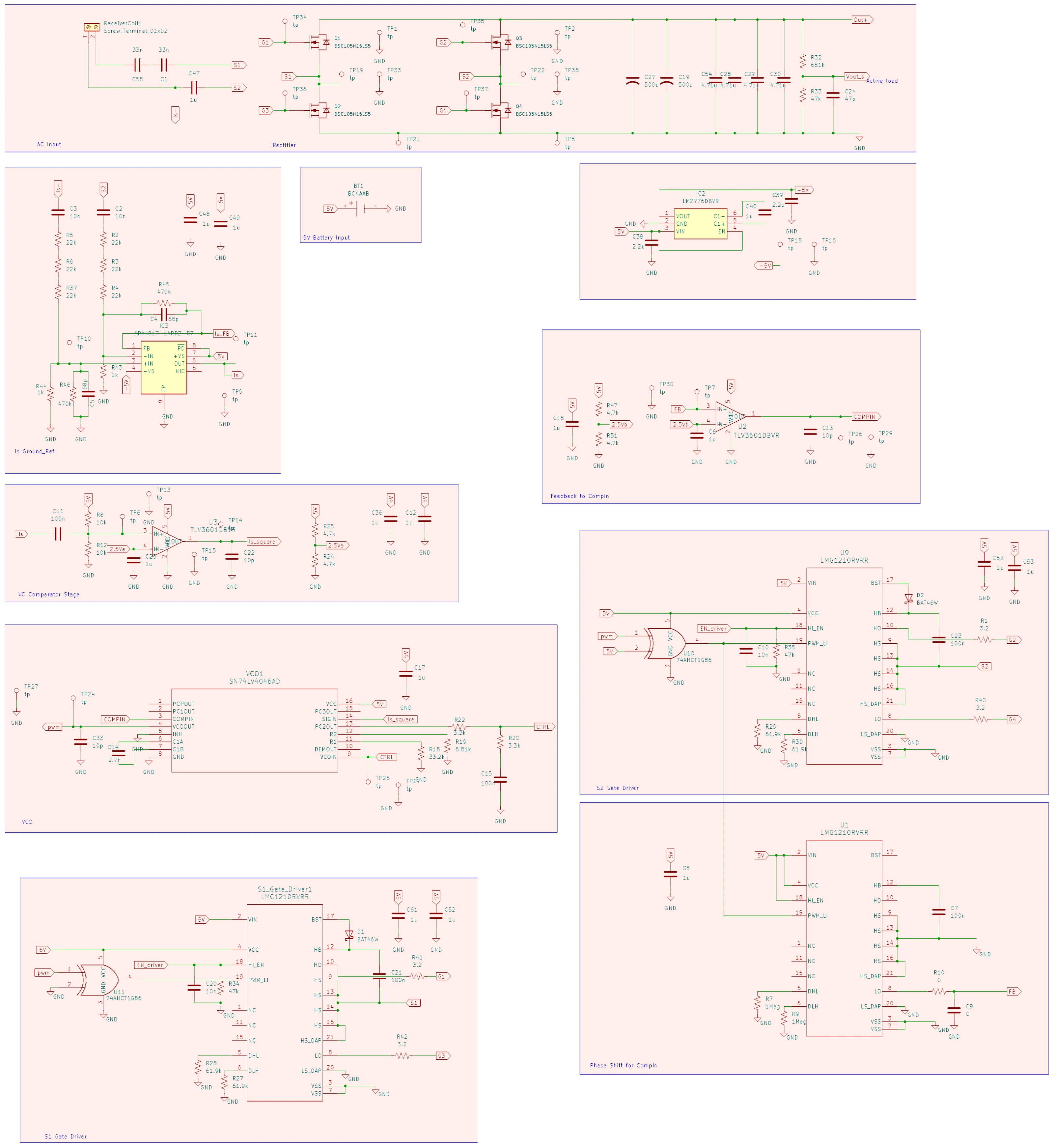
The receiver board: a full bridge of four Infineon BSC105N15LS5 MOSFETs switched in sync with the receiver's AC current, cutting the conduction loss that a diode bridge would waste at 20 A. The KiCad schematic is drawn and being checked in LTspice; board layout comes next.

- Current sensing (ADA4817 amplifier) feeds fast TLV3601 comparators that turn the sensed signals into clean logic edges.
- An SN74LV4046 phase-locked loop tracks the receiver's switching frequency, with a phase-shift stage to time the gate signals.
- Two LMG1210 half-bridge drivers switch the bridge, a third serves the phase-shift stage, and an LM2776 makes the −5 V rail.
- Screw-terminal connection to the receiver coil, a 5 V battery input for the control electronics, and test points throughout for bring-up.
LTspice simulation
Before layout, the rectifier's sensing and gate-timing loop is being checked in LTspice with the vendor models for the parts on the board: ADA4817, TLV3601, 74HC4046, LMG1210 and SN74LVC1G86. The receiver is modeled as a 250 kHz source driving its series-resonant tank (24.68 µH with two 33 nF capacitors), and the circuit is built up in three steps.
| Step | What it adds | Status |
|---|---|---|
| 1. Diode-bridge baseline | Diode bridge into 100 µF and a 50 Ω test load; 0.2 Ω current shunt, ADA4817 amplifier and TLV3601 comparator | Runs: 37.9 V out, ±1.28 A coil current, clean comparator edges |
| 2. Synchronous switching | Diodes replaced by switches (10.9 mΩ on, 580 pF output capacitance); 74HC4046 PLL locks the gate signal to the comparator; 10 ns dead time and 20 ns gate delay | Runs, but the loop hasn't settled yet; resistor values are being re-tuned from the waveforms |
| 3. 6.78 MHz version | The same loop at 6.78 MHz with LMG1210 gate-driver models, XOR gates and a retuned tank | Set up, not yet run |
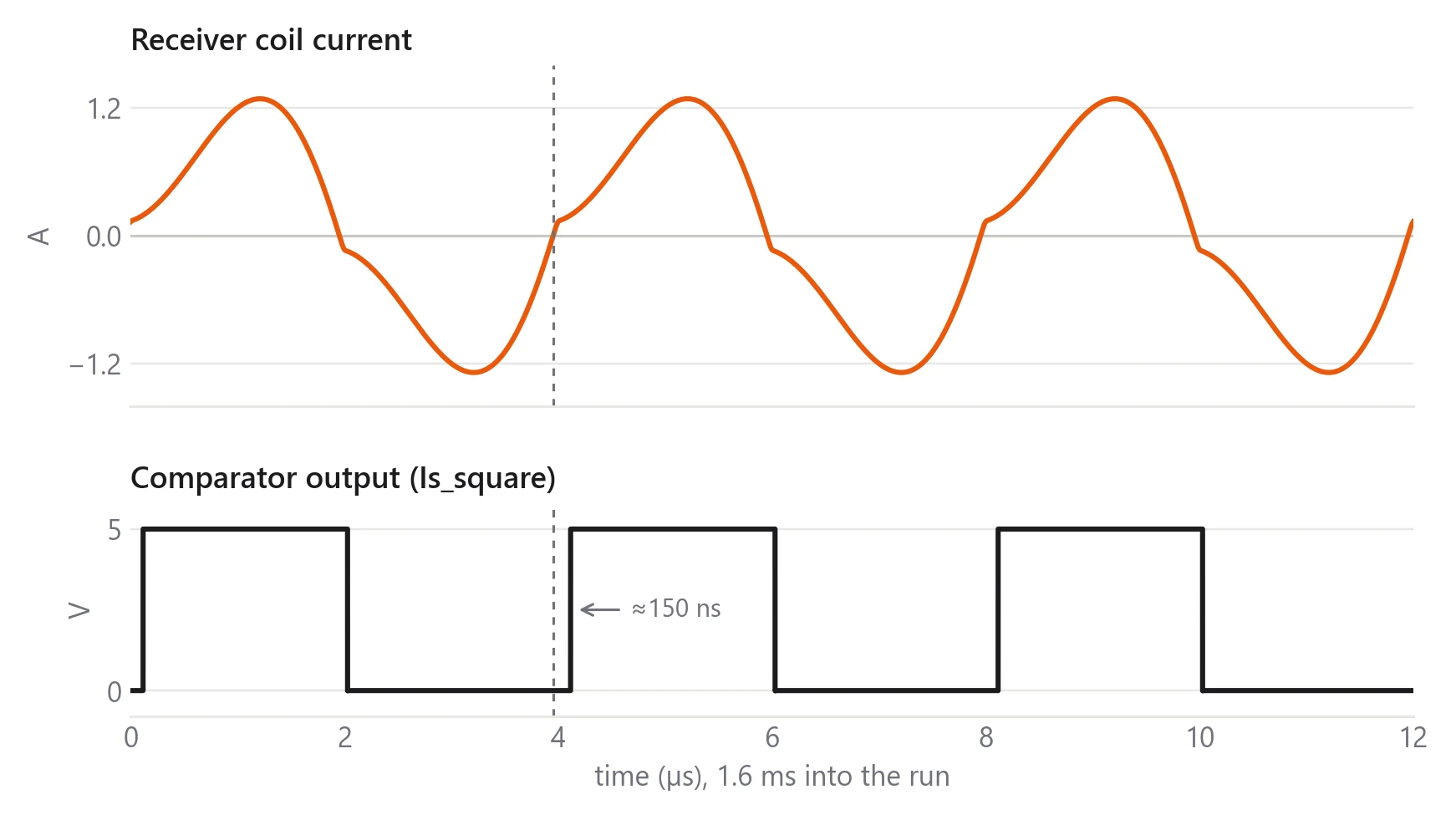
- The MOSFETs need to switch at the current's zero crossings, so that sensing delay (2–4% of the 4 µs period) has to be built into the gate timing.
- The gate logic holds 10 ns of dead time between the top and bottom switch in each leg, so the two are never on at the same time.